 |
| January 20, 2015 | Volume 11 Issue 03 |
Software News & Products
Designfax weekly eMagazine

Archives
Partners
Manufacturing Center
Product Spotlight
Modern Applications News
Metalworking Ideas For
Today's Job Shops
Tooling and Production
Strategies for large
metalworking plants
hyperMILL 2024 CAD/CAM software suite
 OPEN MIND Technologies has introduced its latest hyperMILL 2024 CAD/CAM software suite, which includes a range of powerful enhancements to its core toolpath capabilities, as well as new functionality for increased NC programming efficiency in applications ranging from 2.5D machining to 5-axis milling. New and enhanced capabilities include: Optimized Deep Hole Drilling, a new algorithm for 3- and 5-axis Rest Machining, an enhanced path layout for the 3D Plane Machining cycle, better error detection, and much more.
Learn more.
Find test data issues faster: AI Anomaly Detector
 It can take months of manual engineering time to detect test data abnormalities. Now the task can be performed in a flash. Artificial intelligence software provider Monolith has developed the industry's first AI-powered Anomaly Detector software that can discover a broad range of issues in test data fast -- measurement or sensor errors, user errors, system malfunctions, or incorrect usage of the system during testing. It does this by automating the process of raw test data inspection to look for potential errors or abnormalities across hundreds of test channels.
Learn more.
Loss-free conversion of 3D/CAD data
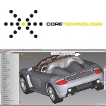 CT CoreTech-nologie has further developed its state-of-the-art CAD converter 3D_Evolution and is now introducing native interfaces for reading Solidedge and writing Nx and Solidworks files. It supports a wide range of formats such as Catia, Nx, Creo, Solidworks, Solidedge, Inventor, Step, and Jt, facilitating smooth interoperability between different systems and collaboration for engineers and designers in development environments with different CAD systems.
Learn more.
Top 5 reasons for solder joint failure
 Solder joint reliability is often a pain point in the design of an electronic system. According to Tyler Ferris at ANSYS, a wide variety of factors affect joint reliability, and any one of them can drastically reduce joint lifetime. Properly identifying and mitigating potential causes during the design and manufacturing process can prevent costly and difficult-to-solve problems later in a product lifecycle.
Read this informative ANSYS blog.
How a BattleBot was built using Onshape
 Learn how RoboGym Robotics, a veteran BattleBots team, said goodbye to Solidworks and took their design game to the next level using Onshape, the cloud-native, all-in-one CAD and PDM solution. RoboGym was able to analyze key components of their Roundhouse BattleBot like its armor and weapon bar, run simulations, collaborate, iterate, and optimize their design to its fullest.
Read this informative Onshape blog.
Trick to measuring angles in SOLIDWORKS
 Learn from the pros at TriMech how to take angle measurements easily in SOLID-WORKS. TriMech has an entire YouTube channel dedicated to SOLIDWORKS tips, and the company is excellent at training too.
View the video.
COMSOL Multiphysics Version 6.2 is here
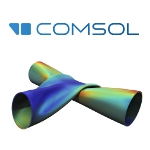 COMSOL Multiphysics Version 6.2 introduces faster solvers for turbulent fluid flow, electric motors, and room acoustics. It also brings data-driven surrogate model functionality for creating multiphysics-based digital twins and building fast and accurate standalone simulation apps. Get the full details of what's new in the latest version.
Learn more.
17 ways SOLIDWORKS 2024 helps you work faster
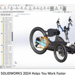 SOLIDWORKS 2024 helps designers and engineers work faster than ever. Learn all about improvements to core 3D CAD modeling features, new 3D modeling techniques, and graphical and software performance boosts that will help you get your parts made and your products developed in record time.
View the video.
6 tips to streamline workflow in Mastercam 2024
 Mastercam 2024 CAD/CAM software has been intentionally upgraded to make programming fast and easy. It prioritizes streamlining workflow so that the entire machining process -- from design to QC -- is as efficient as possible. Learn how to maximize the benefits of Mastercam 2024, including special toolpaths, easier hole-making operations, wireframe shortcuts, and more.
Read this informative Mastercam blog.
How CT data analysis is helping TE Connectivity reach their goal of end-to-end quality inspection
 In a bid to cut their mold and part development process to 25% of the time it took in the past, TE Connectivity has taken ambitious steps to interconnect design and simulation with quality measurement. Learn how the company, in collaboration with PTC (Creo) and Volume Graphics, has worked to ensure as-designed parts match as-manufactured parts as early in the process as possible. An in-depth and illuminating read.
Read the full article.
State-of-the-art mesh morphing technology for super optimization: Ansys and RBF Morph join forces
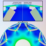 After a long and successful OEM partnership with Ansys, mesh morphing pioneer RBF Morph has two proprietary products featured among the world simulation leader's offerings: Ansys RBF Morph Fluids and Ansys RBF Morph Structures. Thanks to mesh morphing, companies can substantially reduce computational time while performing highly automated design optimization analysis, increasing products' reliability and performance while cutting costs, delivery time, and environmental impact.
Read the full article.
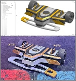
Top Tech Tip: Creating drafts with the rib feature in Onshape
 Ribs are used to add stiffness and strength to parts without adding excessive weight or increasing wall thickness -- most commonly in molded parts that require a draft angle so the part can release from the mold. See the basics of how this is done in Onshape, which features the power of cloud computing, real-time collaboration tools, and a built-in PDM system -- all for the same price as CAD.
Learn more.
How to design a spoon with subdivision modeling: SOLIDWORKS xShape
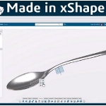 Learn how to design a spoon with SOLIDWORKS xShape, which is found in 3D Sculptor on the 3DEXPERI-ENCE platform. xShape is a next-gen subdivision modeling tool that runs entirely in your browser and takes a freeform approach to creating complex shapes and surfaces. You can design 100% in the cloud or seamlessly integrate your xShape models with your SOLIDWORKS designs. Follow along with this 7-minute tutorial to see what it's all about.
View the video.
What's new in Onshape?
 Check out the latest updates to Onshape, the cloud-native product development platform that delivers professional-grade CAD capabilities with next-gen product data management. New features include customizable keyboard shortcuts, better BOM navigation, improved drawing tools, and new Learning Center content. With Onshape, users can innovate quickly while simultaneously or asynchronously collaborating with other stakeholders on any web-connected device.
View the video.
Open-access learning center for multiphysics modeling
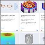 COMSOL, the developer of the COMSOL Multiphysics simulation software, has introduced a new online resource that provides no-cost, open access to modeling and simulation learning material across all areas of physics. Designed with the user in mind, the Learning Center offers a single entry point for users of all skill levels, where courses, articles, and videos present a clear path for learning how to use COMSOL Multiphysics for modeling and simulation.
Check out the COMSOL Learning Center.
Contact lens merges plastics, active electronics via 3D printing
As part of a project demonstrating new 3D-printing techniques, Princeton researchers have embedded tiny light-emitting diodes into a standard contact lens, allowing the device to project beams of colored light.
Michael McAlpine, the lead researcher, cautioned that the lens is not designed for actual use -- for one, it requires an external power supply. Instead, he said the team created the device to demonstrate the ability to "3D print" electronics into complex shapes and materials.

Michael McAlpine, an assistant professor of mechanical and aerospace engineering at Princeton, is leading a research team that uses 3D printing to create complex electronics devices such as this light-emitting diode, shown here printed on curved glass. [Photos by Frank Wojciechowski]
"This shows that we can use 3D printing to create complex electronics including semiconductors," said McAlpine, an assistant professor of mechanical and aerospace engineering. "We were able to 3D print an entire device, in this case an LED."
The hard contact lens is made of plastic. The researchers used tiny crystals, called quantum dots, to create the LEDs that generated the colored light. Different size dots can be used to generate various colors.
"We used the quantum dots [also known as nanoparticles] as an ink," McAlpine said. "We were able to generate two different colors: orange and green."
The contact lens is also part of an ongoing effort to use 3D printing to assemble diverse, and often hard-to-combine, materials into functioning devices. In the recent past, a team of Princeton professors including McAlpine created a bionic ear out of living cells with an embedded antenna that could receive radio signals.
Yong Lin Kong, a researcher on both projects, said the bionic ear presented a different type of challenge.
"The main focus of the bionic ear project was to demonstrate the merger of electronics and biological materials," said Kong, a graduate student in mechanical and aerospace engineering.
Kong, the lead author of the Oct. 31 article describing the current work in the journal Nano Letters, said that the contact lens project, on the other hand, involved the printing of active electronics using diverse materials. The materials were often mechanically, chemically, or thermally incompatible -- for example, using heat to shape one material could inadvertently destroy another material in close proximity. The team had to find ways to handle these incompatibilities and also had to develop new methods to print electronics, rather than use the techniques commonly used in the electronics industry.
"For example, it is not trivial to pattern a thin and uniform coating of nanoparticles and polymers without the involvement of conventional microfabrication techniques, yet the thickness and uniformity of the printed films are two of the critical parameters that determine the performance and yield of the printed active device," Kong said.

McAlpine and Yong Lin Kong, a graduate student in mechanical and aerospace engineering, use a custom-built 3D printer to create the electronics described in their research.
McAlpine said that one of 3D printing's greatest strengths is its ability to create electronics in complex forms. Unlike traditional electronics manufacturing, which builds circuits in flat assemblies and then stacks them into three dimensions, 3D printers can create vertical structures as easily as horizontal ones.
"In this case, we had a cube of LEDs," he said. "Some of the wiring was vertical and some was horizontal."
To conduct the research, the team built a new type of 3D printer that McAlpine described as "somewhere between off-the-shelf and really fancy." Dan Steingart, an assistant professor of mechanical and aerospace engineering and the Andlinger Center, helped design and build the new printer, which McAlpine estimated cost in the neighborhood of $20,000.
McAlpine said that he does not envision 3D printing replacing traditional manufacturing in electronics any time soon; instead, they are complementary technologies with very different strengths. Traditional manufacturing, which uses lithography to create electronic components, is a fast and efficient way to make multiple copies with a very high reliability. Manufacturers are using 3D printing, which is slow but easy to change and customize, to create molds and patterns for rapid prototyping.
Prime uses for 3D printing are situations that demand flexibility and that need to be tailored to a specific use. For example, conventional manufacturing techniques are not practical for medical devices that need to be fit to a patient's particular shape or devices that require the blending of unusual materials in customized ways.
"Trying to print a cellphone is probably not the way to go," McAlpine said. "It is customization that gives the power to 3D printing."
In this case, the researchers were able to custom 3D print electronics on a contact lens by first scanning the lens, and feeding the geometric information back into the printer. This allowed for conformal 3D printing of an LED on the contact lens.
Besides McAlpine, Kong, Tamargo, Kim, Rand, and Steingart, the researchers involved in the project included postdoctoral researchers Blake Johnson, Maneesh Gupta, and Tae-Wook Koh, and graduate student Huai-An Chin.
Support for the project was provided by the Air Force Office of Scientific Research and the Defense Advanced Research Projects Agency
Source: Princeton University
Published January 2015
Rate this article
View our terms of use and privacy policy